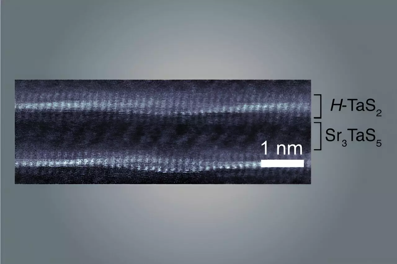
Recent advancements in materials science, particularly in the realm of superconductors and quantum materials, have unveiled a fascinating new material crafted by physicists at the Massachusetts Institute of Technology (MIT) and their collaborators. Characterized by an intricate arrangement of wavy atomic layers, this innovative substance not only challenges our understanding of conventional crystalline structures but also opens doors to myriad applications due to its unique properties.
At its core, this new material is formed by alternating layers of tantalum and sulfur that are interspersed with “spacer” layers comprised of strontium, tantalum, and sulfur. The distinctive wavy texture of these atomic layers is not merely an aesthetic feature; it plays a critical role in facilitating the material’s superconductive characteristics. The creation of these wavy formations stems from an inherent mismatch in the sizes and structures of the crystal lattices of the various layers. This structural misalignment results in a buckling phenomenon analogous to stacking two sheets of paper of differing sizes, creating a complex interplay of atomic forces. Thus, when the layers are assembled and heated properly, they generate intrinsic wave-like patterns that mark the material’s uniqueness.
The significance of these waves extends far beyond structural novelty; they significantly influence the behavior of electrons moving through the material. As researchers led by physicist Joseph Checkelsky demonstrate, these small but consequential waves enable electrons to traverse pathways that are more favorable energetically. The electrons are forced into a “preferred” direction owing to the channeling effect of the wave structure, meaning that they encounter less resistance as they flow through the valleys between corrugated layers. This transformation in electron dynamics is pivotal in unlocking the material’s superconductivity and unique metallic properties.
One of the hallmark features of this research is the methodical, rational design approach that the team employed to synthesize the material. Unlike many typical material synthesis methods that rely heavily on trial and error, the researchers developed the new material with a clear understanding of atomic interactions and the behaviors inherent to the materials being manipulated. As highlighted by Aravind Devarakonda, lead author of the study, the team’s methodology involved mixing relevant powders, subjecting them to high temperatures, and harnessing the results of subsequent chemical reactions to yield a material with macroscopic manipulation capabilities.
The paradigm shift towards rational design does not only improve the efficacy of the synthesis process; it also lays the groundwork for future discoveries. The researchers express confidence that their successes with this new material form the basis for creating even more advanced compounds with unconventional properties. This realization showcases the potential for an entire new class of advanced materials, departing from conventional methodologies and venturing into uncharted scientific territories.
The implications of this breakthrough extend beyond academic curiosity. The unique superconducting properties exhibited by the material, coupled with its macroscopic size, signal promising applications in fields ranging from quantum computing to advanced electronics. Historically, the challenge with two-dimensional materials akin to this wavy creation has been their minuscule size, posing significant hurdles to manipulation and experimentation. However, by producing materials that are large enough to be handled comfortably, researchers are poised to explore a variety of practical applications that were previously limited by size constraints.
The team’s discovery also raises intriguing questions about the behavior of condensed matter systems. The anomalous behaviors observed in their experiments—such as the varying strengths of superconductivity across the material—represent a unique opportunity for physicists to delve deeper into the understanding of quantum phenomena. As Devarakonda metaphorically puts it, the researchers have “planted the flag” in this new territory, setting the stage for future explorations that may yield unexpected and revolutionary findings.
As the field of materials science continues to evolve, the creation of this wavy atomic structure marks a significant milestone in our quest to understand and manipulate matter at the quantum level. With the goal of expanding the boundaries of what is possible with superconductors and other advanced materials, the MIT team’s work has not only contributed a novel material but has also bolstered the foundational principles guiding future innovations.
The development of this novel material demonstrates that a combination of scientific insight, creative methodology, and innovative thinking can lead to breakthroughs with far-reaching implications. As we stand on the cusp of a new era defined by the clever manipulation of atomic structures, the scientific community looks forward to the myriad applications that this exciting research may foster—transforming our understanding of materials science and potentially reshaping the technological landscape of the future.

