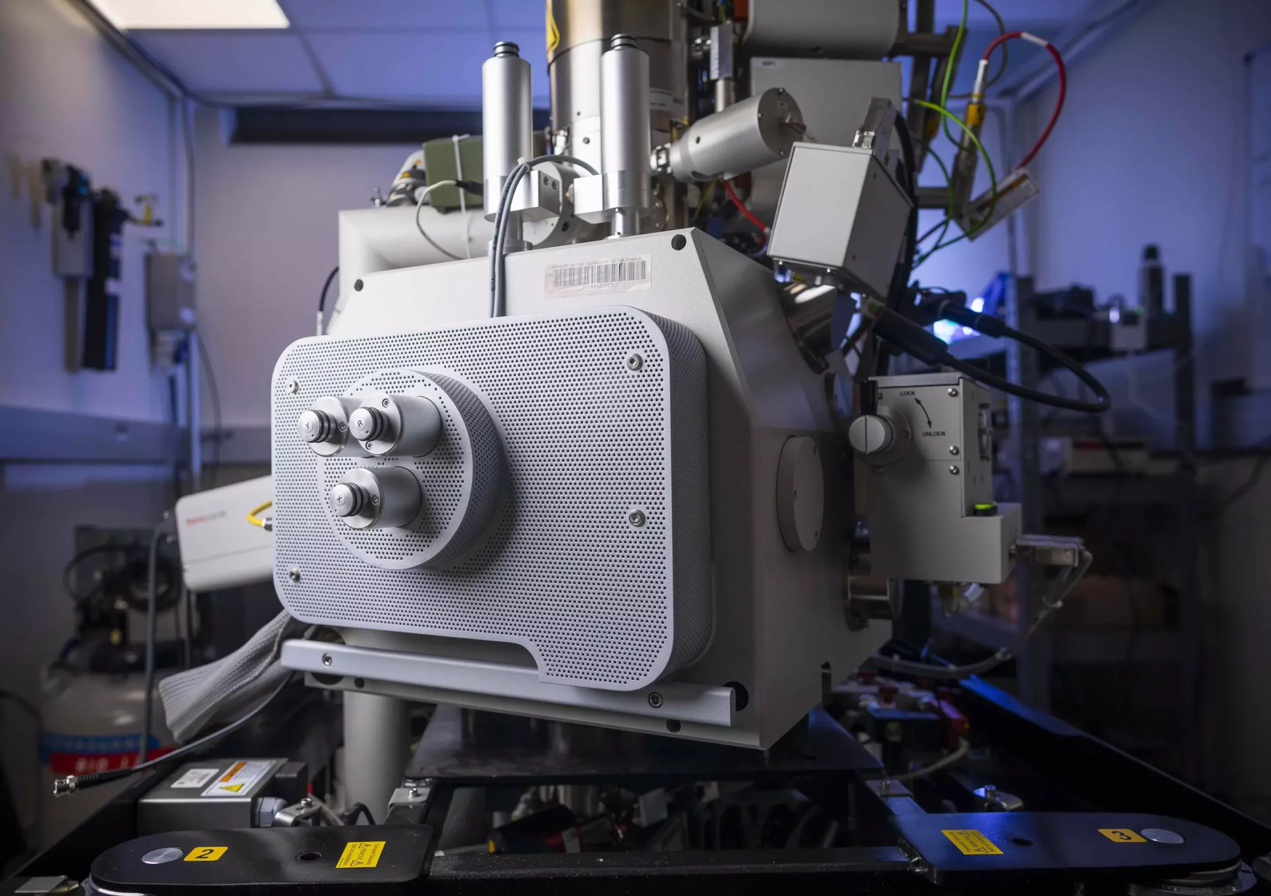
In a remarkable scientific advancement, researchers from UC Santa Barbara have unveiled a pioneering technique that visualizes electric charges moving across semiconductor interfaces—a phenomenon that has often been relegated to theoretical discussions in textbooks. By leveraging the novel scanning ultrafast electron microscopy (SUEM) methods, developed in Bolin Liao’s laboratory, they have accomplished what was previously thought to be an elusive task: the direct observation of this fleeting process. Liao, an associate professor of mechanical engineering, highlights the importance of this breakthrough, emphasizing that it not only challenges existing theories but also validates indirect measurements taken in the field of semiconductor science.
At the heart of this research lie photocarriers—charged entities generated when sunlight strikes semiconductor materials like silicon and germanium. These carriers, through their movement and separation from equivalent negative charge “holes,” create electrical energy that can be harnessed for various electronic applications, including solar energy. However, the efficiency of photovoltaic technologies is stunted as these hot photocarriers lose their energy in mere picoseconds, releasing most of their initial energy as waste heat. Given that such rapid energy loss limits energy conversion efficiency, understanding hot carrier behavior during this cooling process and their migration across heterojunctions is crucial in the quest for more effective semiconductor materials.
Liao and his team concentrated their research on the silicon-germanium heterojunction, a blend of well-established semiconductor materials often used in solar cells and telecommunication devices. Their work goes beyond basic theoretical premises, aiming to enhance our comprehension of how hot carriers navigate through interfaces—a vital component in the design and efficiency of future devices.
One of the primary innovations in this study stems from the use of SUEM, which grants researchers unprecedented temporal resolution in depicting how these carriers flow across semiconductor boundaries. By employing picosecond-scale laser pulses as an optical shutter, researchers can observe rapid events following the generation of hot carriers. Liao asserted that this technique allows scientists to capture and visualize the behavior of electrical charges during that critical nanosecond timeframe—information that was previously only speculated upon.
The experimental results reveal an intricate dynamic where hot carriers, initially zipping through semiconductor materials at astonishing speeds due to their heightened energy, behave differently when they meet junctions. A considerable number of these carriers encounter trapping potentials at the junction interface, which impedes their mobility and can hinder device performance—a phenomenon that, while understood through semiconductor principles, is strikingly captured for the first time in practice.
The practical implications of this research are profound, especially as they open new avenues for optimizing semiconductor devices. The visualization of charge trapping at junctions signals a critical insight that device engineers must acknowledge to enhance performance and efficiency. Liao emphasized that recognizing and addressing these effects could transform future semiconductor applications, making them more efficient at harnessing energy.
Furthermore, this exploration contributes to a rich history of semiconductor research at UC Santa Barbara, aligning with the legacy of the late Professor Herb Kroemer. The pioneering work of Kroemer—who first proposed the concept of heterostructures in 1957—remains foundational to the explosion of microchip and computing technologies. This research not only reinforces Kroemer’s vision that “the interface is the device” but also demonstrates the enduring relevance of heterojunctions in addressing modern semiconductor challenges.
As UC Santa Barbara’s researchers illustrate new mechanisms behind charge transport in semiconductors, the scientific community stands on the brink of significant advancements in energy efficiency and material performance. This innovative work undoubtedly sets a new standard for semiconductor research, providing a fresh perspective that could lead to transformative technologies across numerous applications. With the ability to visually track hot photocarrier activity, the pathway to next-generation electronic devices appears brighter than ever, paving the way for more sustainable and effective solutions in the realm of energy and electronics. The future of semiconductor technology seems promising, bolstered by an increasingly nuanced understanding of material behavior at the quantum level.

